|
Key highlights
- India’s Semiconductor Mission
- Design Linked Incentive (DLI)
- Production Linked Incentive (PLI)
- Drawbacks
- Global Leadership Goal
- Future Directions
|
The Design Linked Incentive (DLI) Scheme aims to offer financial incentives as well as design infrastructure support across various stages of development and deployment in India. The article explains the conceptualisation of India’s Design Linked Incentive (DLI) Scheme as one that aims at supporting the semiconductor design ecosystem by encouraging startups and micro, small, and medium enterprises (MSMEs) and academic institutions. It outlines the scheme's structural framework, the objectives articulated, and how the scheme would contribute to the improvement of innovation, intellectual property generation, and global competitiveness, although systemic issues like talent shortage and poor infrastructure would also be addressed. By doing so, it would make India an upcoming global semiconductor design hub.

|
Tips for Aspirants
The article is relevant to the UPSC CSE and State PSC examinations since it supplements the understanding of the Indian semiconductor policy, governing institutions, tech innovation, and strategic self-sufficiency of the country as some of the important themes in the realms of economy and technologies.
|
|
Relevant Suggestions for UPSC and State PCS Exam
- The digital economy, national security, and technological autonomy cannot do without semiconductors.
- Semiconductor components are also imported at around 90%, thus highlighting weak spots in supply chains.
- Design Linked Incentive (DLI) Scheme was launched in 2021 as a part of the India Semiconductor Mission and is complemented by the 76,000-crore Production Linked Incentive (PLI) scheme.
- The scheme has been aimed at assisting startups and MSMEs, providing electronic design automation (EDA) tools, encouragement of the creation of intellectual property, and incubation of at least twenty domestic design firms.
- According to the latest reports, ninety-five companies have utilized EDA tools; 24 design projects have been approved; 16 tape-outs, six ASIC chips, and 10 patents have been filed; and over 1,000 engineers have been engaged.
- The major threats are the lack of skilled talent, infrastructural bottlenecks, the increasing competition in the global arena, and the necessity of long-term investment.
- The promotion of skills, creating innovation centres, encouraging partnerships between the industries, and presence in the global value chains are related solutions in making India one of the leading centres of semiconductor design.
|
The semiconductor has emerged as the primary established pillar of the global digital economy, with the advancements in artificial intelligence, cost, telecommunication, defence, and consumer electronics. In the case of India, creating a sound semiconductor environment is a strategic priority that is closely connected with national security and technological autonomy, as well as economic competitiveness. India has traditionally been very skilled in end-to-end software and information technology services, but there has been a limit in any interaction with semiconductor design and production. Realizing this gap, the Government of India has introduced the DLI Scheme- a policy intervention to stimulate local potential in semiconductor design. The initiative is to foster the growth of startups, MSMEs, and academic institutions with monetary support, development, and infrastructure of designs, and linking them to market access. Relationships through the DLI Scheme have the aim of raising India to the semiconductor design excellence hub by fostering innovations, creation of intellectual property, and the need for industry hatched to join in-the-cycle supply chain. In addition to short-term economic benefits, the project represents a long-term perspective of reducing the reliance on imports, strengthening the supply-chain resilience, and empowering India to be substantively involved in the geopolitics of technology. This article raises a critical question about the structure, goals, and transformability of the scheme, while discussing the current issues and offering future opportunities for the development of the ecosystem of semiconductor design in India.
Introduction & Context of the DLI Scheme
India's Design Linked Incentive (DLI) Scheme is a cornerstone of its semiconductor strategy, offering financial support (up to 50% of costs) and design tools to boost domestic chip design, IP creation, and innovation by startups, MSMEs, and academia, aiming to reduce import reliance, build a robust ecosystem, and develop critical indigenous chips for sectors like telecom, defense, and IoT, positioning India as a global semiconductor hub.
Semiconductor interests in India have been motivated by the fact that integrated circuits are the fabric of modern digital systems, which provide capabilities of both mobile communications and essential defense systems. Design Linked Incentive (DLI) Scheme is a strategic policy intervention that will enhance the speed at which indigenous design capabilities are stimulated and reduce dependence on imported technologies.
Global Significance
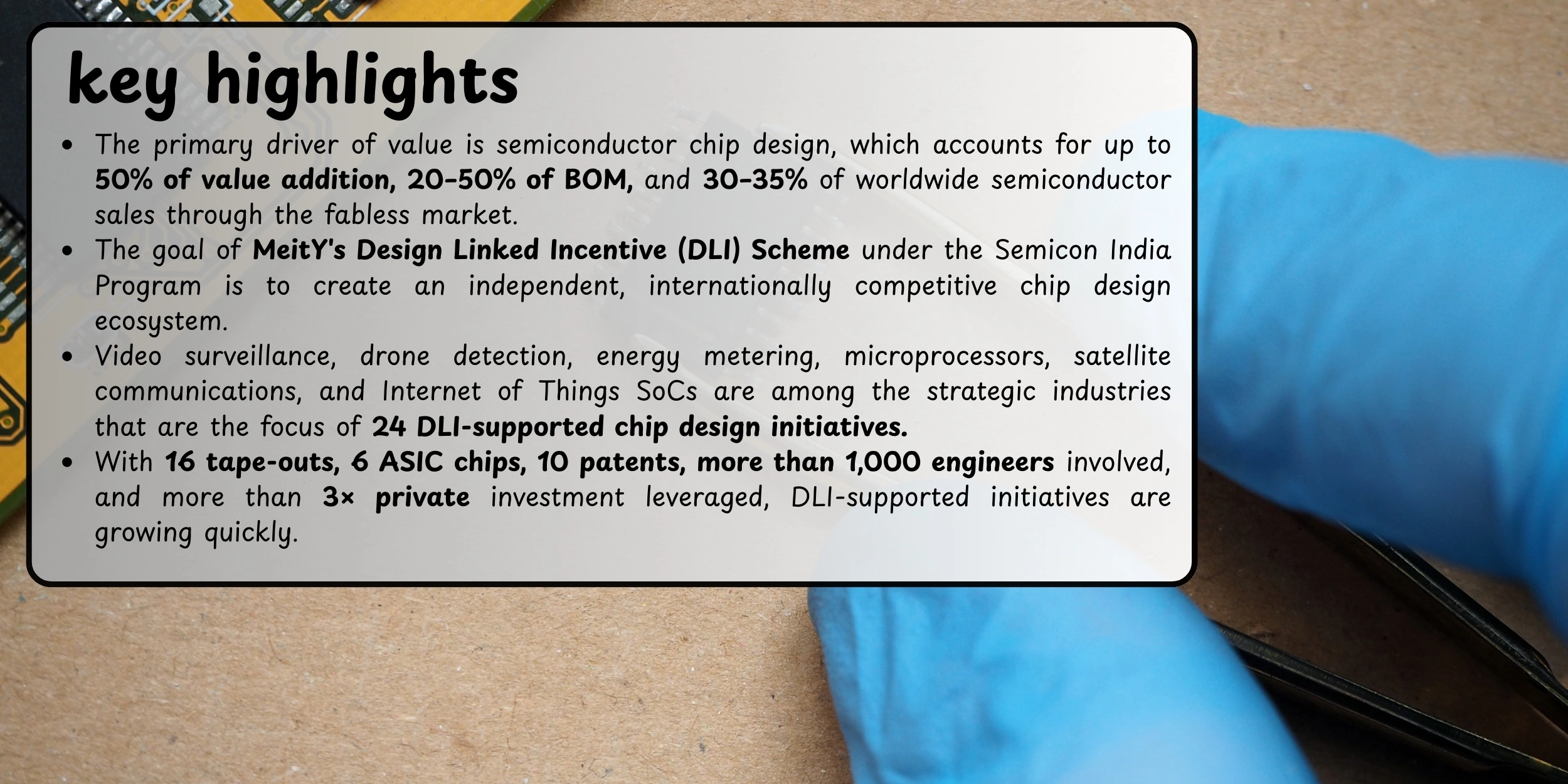
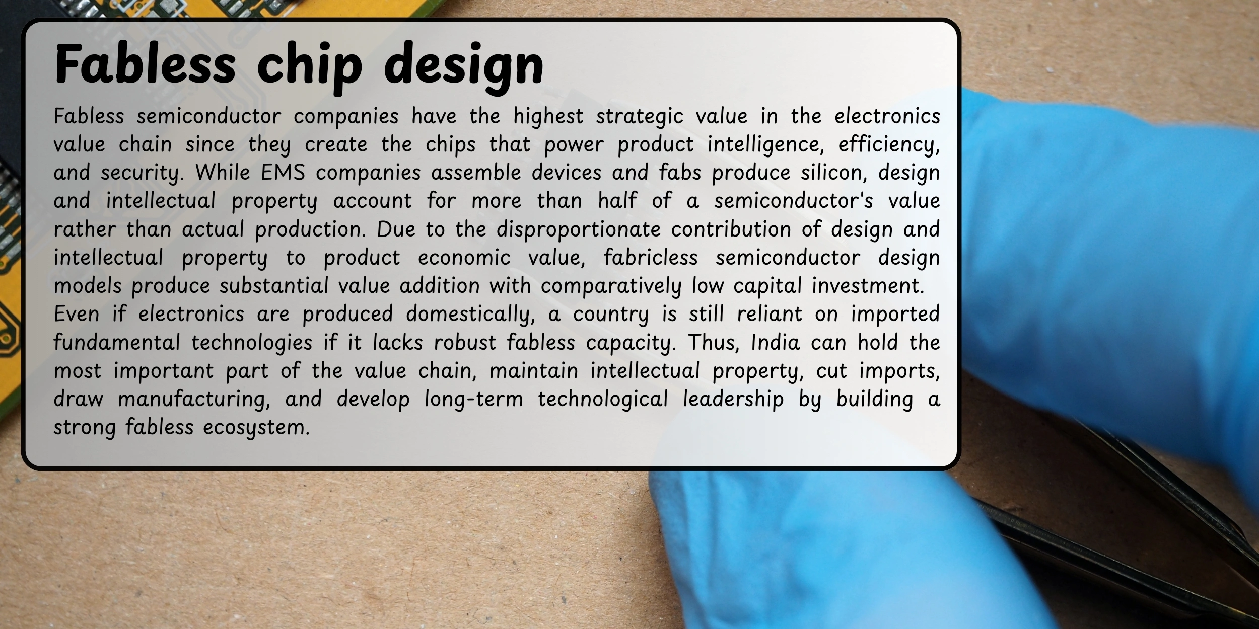
Semiconductors are the key facilitators of economic growth, national security, and technological self-determination. At a worldwide level, the design stage adds nearly 50 percent of the value being created in the semiconductor supply device, and fabless design companies provide 30-35 percent of semiconductor profits worldwide. In the case of India, it is necessary to expand the domestic design capabilities in order to gain significant access to this high-value segment.
India’s Policy Context
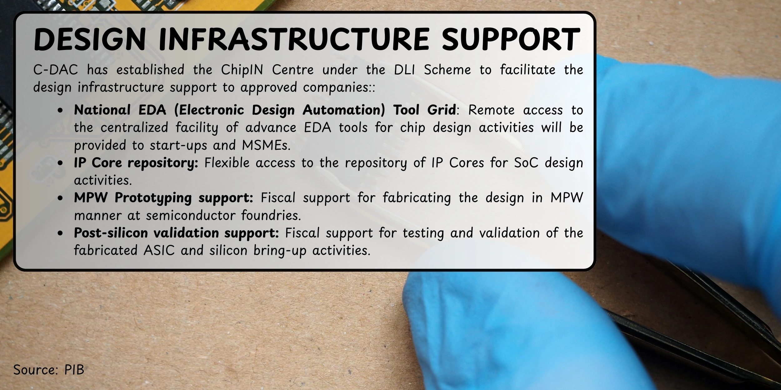
The semiconductor future of India was given a major boost with the launch of an India Semiconductor Mission (ISM) in 2021, as part of the Semicon India Programme. The DLI initiative is a supplementary program to the 76,000-crore Production Linked Incentive (PLI) scheme; it is designed to focus on design innovation. It offers financial assistance, Electronic Design Automation (EDA) solutions, multi-project wafer fabrication services, and post-silicon validation services. This policy ecosystem aligns with the National Policy on Electronics 2019, which puts an idea of making India a global centre in Electronics System Design and Manufacturing (ESDM).
The DLI Scheme-
Recent data portray physical gains that can be traced to the scheme. By early 2026, the government has approved 24 chip-projects in fields that include video surveillance, drone-detecting, energy metering, microprocessors, satellite communications, and Internet-of-Things Systems-on-Chip (SoCs). Further, 95 companies have access to EDA tools at an industry level, which considerably lowers the start-up costs in infrastructure. It already had 16 tape-outs, 6 ASIC chips, 10 patents, employed more than 1,000 engineers, and received over three times the amount of private investment. These results highlight the driving effect of the DLI in fostering creativity and innovation of intellectual-property.
Strategic Importance to India
The DLI Scheme is more than an economic program, and it is an imperative strategy. India hopes to check reliance on foreign technologies, promote the resilience of the supply chains, and increase its position in the global semiconductor geopolitics by promoting native design. With increased digital penetration, semiconductors will be the essential building block in some of the key industries, such as healthcare, transportation, defense, and space exploration. This design hub in India will ensure long-term competitiveness and is consistent with the broader vision of Atmanirbhar Bharat.
Framework and Objectives of the DLI Scheme
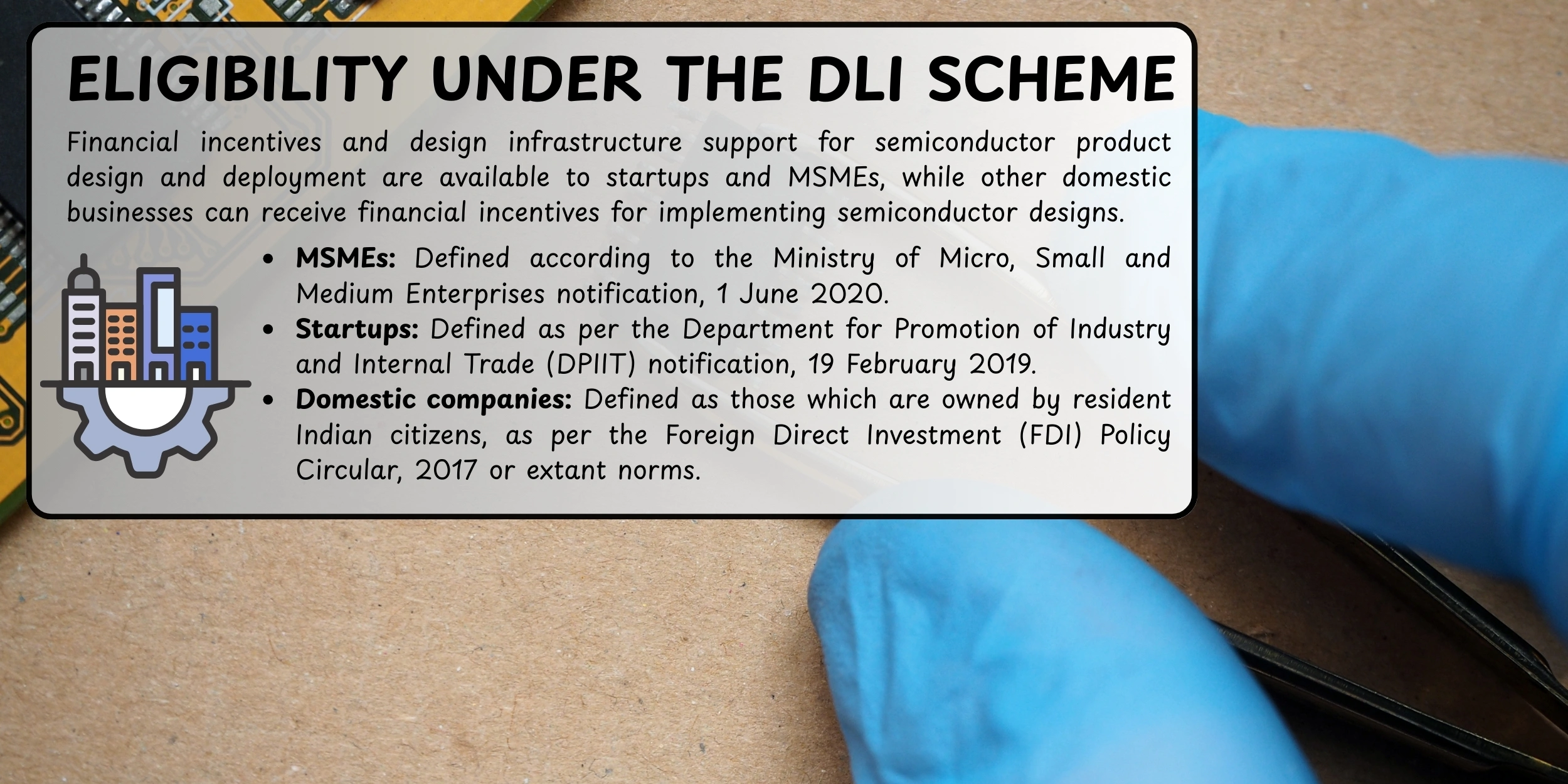
Design Linked Incentive (DLI) Scheme is a critical component of the Indian semiconductor mission, which is designed to strengthen the native chip design capacity. It supports startups, micro, small, and medium enterprises (MSMEs), and academic institutions financially and strategically.
Policy Framework
It was launched in December 2021 under the India Semiconductor Mission (ISM). Within a five-year timeframe, it provides financial incentives and design incentives and infrastructure support in Integrated Circuits (ICs), Chipsets, Systems-on-Chip (Socs), or semiconductor-linked intellectual property (IP) cores. The programme is part of the larger Production Linked Incentive (PLI), 76,000-crore programme, but focuses more on design innovation, not production.
Objectives of the Scheme
These are the main goals that include:
- To support domestic design businesses through a system to refund 50 percent or less of approved project expenses.
- To access the state-of-the-art Electronic Design Automation (EDA) software, multi-venture wafer fabrication and post-silicon validation equipment.
- This is to encourage intellectual-property creation, hence decrease reliance on foreign technologies, to bolster the place of India in semiconductor supply chains around the world.
Target Beneficiaries
The plan is startup-friendly, MSME-friendly, and academic-friendly, and at least 20 domestic semiconductor design companies are to be incubated. It aims to create a chip design democratic approach and encourage innovation in many different industries by reducing the barrier to entry, which includes Internet of Things (IoT), autonomous vehicle advancements, defence, and telecommunications.
Emerging Outcomes
By 2025, the DLI Scheme had enabled 95 companies to access industry-grade EDA tools, 24 chip-design projects and also 16 tape-outs, 6 ASIC chips and 10 patents. The number of engineers involved has increased by more than 1,000, and the multiplication of investments made by the individuals thus shows the catalytic effect brought about by the initiative.
Strategic Significance
DLI Scheme is not just a financial programme but a strategic intervention which aims at making India a global destination when it comes to Electronics System Design and Manufacturing (ESDM). Through the indigenous design, India aims at increasing the resilience of the supply chain, reducing the reliance on imports, and technologies sovereignty. This is in line with the general direction of the vision of Atmanirbhar Bharat and the desire of India to become a powerhouse in semiconductor design.
Ecosystem Growth under the DLI Scheme
The Indian semiconductor ambitions are not restricted to fiscal incentives; the Design Linked Incentive (DLI) scheme aims at stimulating a holistic ecosystem, which integrates innovation, infrastructure, and human capital so as to generate sustainable development.
1. Enhancing the Infrastructure of Innovation
An important aspect of ecosystem development is the provision of high-level design infrastructure. In the DLI Scheme, ninety-five companies have obtained access to industry-level Electronic Design Automation (EDA) tools, which has made start-ups and MSMEs accessibility easier. Such common infrastructure costs less, speeds up the prototyping process, and makes participation in chip design a democratic process so that innovation is not restricted to big corporations.
2. Increasing Portfolio of projects
The scheme has already funded twenty-four chip design projects in many fields, including video surveillance, drone detection, energy metering, microprocessors, satellite communications, and Internet-of- Things Systems-on-Chip (IoT SoCs). These initiatives demonstrate the strategic nature of India in the areas that are of critical interest to the country and digital transformation. The scheming of applications is an indication that the DLI Scheme is more relevant to the development of an ecosystem based on a wide base, rather than focusing on a technological niche.
3. Talent Creation and Employment
The key aspect of ecosystem development is human capital. DLI-supported projects have employed more than one thousand engineers to help them develop their skills and secure jobs. The scheme has created a pipeline of competent individuals who can spearhead innovation within the semiconductor design industry by connecting academics, start-ups, and industry. This pool of talent is also necessary to generate long-term competitiveness and reduce dependence on foreign skills.
4. Intellectual Property
Intellectual property creation is also observable in the ecosystem, where ten patents have been registered so far, sixteen tape-outs, and six ASIC chips have been developed with the assistance of DLI. Moreover, the scheme has used more than three times the amount of private investment than government funding, highlighting its catalytic position in attracting investment and creating confidence among the investors. These results promote the scheme to generate innovation as well as financial sustainability.
5. Ecosystem Integration
Besides the short-term production, the DLI Scheme is also positioning India in semiconductor supply chains across the world. It was able to create local design capacities, which means that India will be less exposed to foreign shocks and enhance its sovereignty in technology. The ecosystem development promoted through the DLI is in tandem with the Semicon India Programme at large and the vision of Atmanirbhar Bharat so that India becomes a world player in semiconductor engineering.
DLI Scheme Challenges & How to Way Forward
Design Linked Incentive (DLI) scheme has significantly spurred the growth of the semiconductor design industry in the country, but there were several substantive issues that have remained and pose a threat to long term sustainability of growth and competitiveness of this sector globally.
Talent Shortages
Semiconductor engineers of an extremely specialised nature are highly lacking in India. The report published by the Indian Electronics and Semiconductor Association (IESA) indicates that the country needs to provide 250, 000 professionals with adequate qualifications by the year 2030, and the current generation is way below these expectations. To overcome this shortage, it is necessary to make large-scale investments in higher-education programs, effective industry-academic collaboration and specialised skills-training programs.
Infrastructure Bottlenecks
Nevertheless, the semiconductor infrastructure in India is still inadequate, though there is an incremental development. Even specialist fabrics facilities and high-tech testing laboratories, as well as reliable supply chains, still remain significantly scarce. According to recent studies, India imports approximately 90 percent of its semiconductor parts and therefore makes the local ecosystem susceptible to shocks experienced in international supply chains. There is thus a necessity to expand the domestic fabrication and validation capacity so as to lessen dependency as well as support resilience.
Global Competition
The aspirations of the semiconductor industry in India take place in a very competitive global environment. Countries like the United States, Taiwan and South Korea have had decades of experience and well-established ecosystems. India has to establish a clear differentiation by focusing on specialised aspects of design such as Internet of Things (IoT) tools, automotive electronics and defence applications that are steadily growing in demand and still highly promising in terms of innovation.
Continuity and Investment-
This should be continued to be supported by policy. Although the DLI scheme has already attracted three times the investment made by the private sector compared to the government funds, long-term success is only guaranteed with consistent incentive schemes, clear regulatory policies and a business climate that ensures ease of doing business. The participation of venture capital and building up partnerships globally will additionally strengthen the semiconductor design ecosystem in India.
How to Way Forward in DLI Scheme?
The future trend requires a complex approach:
- Curtaining skills: semiconductor-oriented curriculum and training centres.
- Expansion of the infrastructure: Development of fabrication and testing facilities through public- private partnership.
- Hubs of Innovation: Form regional centres to promote interaction between start-ups, academic institutions and companies.
- Integration: Become a reliable provider of semiconductors in the world supply chains.
Conclusion
Design Linked Incentive (DLI) Scheme is one of the key stepping blocks in India's quest to be technologically independent and to also aspire to sit at a top position in the semiconductor world. The scheme strengthens the principles of long-term ecosystem through indigenous design opportunities, promoting the emergence of new companies, and accelerating the emergence of intellectual property. Despite the challenges that still exist in respect to the acquisition of talents, the development of infrastructure, and international struggles, a long term policy support and strategic investment have the potential to turn these limitations around into opportunities. As part of the wider Semicon India Programme and to support the Atmanirbhar Bharat vision, the DLI Scheme highlights India's desire to emerge as a competent global hub for semiconductor design, thus driving innovation, economic enhancement, and the sustainability of the country's security in the long term.