UPSC Current Affairs
CHIPS TO STARTUP PROGRAM
Background and strategic context Semiconductors have become a strategic foundation for economic growth, technological leadership, and national security. Global demand for advanced electronics, AI systems, and digital infrastructure is rising rapidly. The global semiconductor industry is projected to reach nearly USD 1 trillion by 2030.
VRAuthor Desk
3 min read
Background and strategic context Semiconductors have become a strategic foundation for economic growth, technological leadership, and national security. Global demand for advanced electronics, AI systems, and digital infrastructure is rising rapidly. The global semiconductor industry is projected to reach nearly USD 1 trillion by 2030.
Background and strategic context
- Semiconductors have become a strategic foundation for economic growth, technological leadership, and national security.
- Global demand for advanced electronics, AI systems, and digital infrastructure is rising rapidly.
- The global semiconductor industry is projected to reach nearly USD 1 trillion by 2030.
- At the same time, the global ecosystem faces a shortage of skilled semiconductor professionals, with a requirement of over 1 million additional experts by 2032.
- This situation places India in a critical position to contribute skilled manpower and indigenous innovation to the global semiconductor value chain.
INDIA’S POLICY RESPONSE
- Recognising chip design as a national strategic priority, the Ministry of Electronics and Information Technology has launched multiple initiatives to strengthen India’s semiconductor ecosystem.
- These initiatives focus on:
- Talent creation
- Indigenous design capability
- Academic–industry collaboration
- Nearly 400 organisations are covered under these efforts, including:
- 305 academic institutions under the Chips to Start-up (C2S) Programe
- 95 startups supported under the Design Linked Incentive (DLI) Scheme
WHAT IS THE CHIPS TO STARTUP PROGRAM?
- C2S is a national capacity-building programme launched in 2022
- Implemented by Ministry of Electronics and Information Technology
- Total outlay: ₹250 crore (5 years)
- Goal:
- Build industry-ready chip designers
- Promote indigenous chip design
- Support self-reliance (Atmanirbhar Bharat)
CORE OBJECTIVES OF C2S
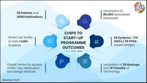
- Train 85,000+ skilled professionals
- Enable hands-on chip design & fabrication
- Encourage:
- Start-ups
- Patents
- IP core development
- Reduce dependence on imported chip technologies
WHO IS BEING TRAINED?
- PhD scholars: 200 (advanced chip research)
- Tech (VLSI / Embedded): 7,000
- Tech (ECE / CS with VLSI focus): 8,800
- Tech students: 69,000
- Total trained / enrolled so far:
- 1 lakh enrolled
- ~67,000 already trained Scale of Participation
- Around 400 organisations involved
- 305 academic institutions (under C2S)
- 95 startups (linked with DLI Scheme)
- Open to students across India, regardless of location
HOW THE PROGRAM WORKS?
- Combines:
- Classroom learning
- Short-term courses
- Labs & projects
- Strong focus on hands-on experience
- Students work on:
- Uses real industry tools and foundries
ROLE OF CHIP IN CENTRE (C-DAC BENGALURU)
- Operated by Centre for Development of Advanced Computing
- Acts as national hub for chip design
- Supports 300+ institutions
- Provides:
- Advanced EDA tools
- Compute infrastructure
- IP libraries
- Technical mentoring
KEY FUNCTIONS
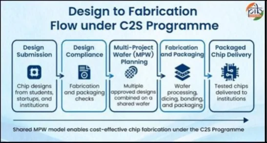
- Collects student chip designs
- Verifies and improves designs
- Sends designs for fabrication every 3 months
- Has resolved 4,800+ technical support requests
FABRICATION SUPPORT-SCL MOHALI
- Fabrication done at Semi-Conductor Laboratory
- Uses 180 nm technology
- Process:
- Multiple student designs combined on a shared wafer
- Chips are fabricated, packaged and returned
- Result:
- Students see their designs on real silicon
INFRASTRUCTURE & COMPUTING TOOLS & LABS
Provided
- SMART Labs (NIELIT)
- FPGA boards (centralised & distributed)
- PARAM Utkarsh supercomputer
MAJOR ACHIEVEMENTS SO FAR
- 1 lakh users used national EDA infrastructure
- 175 lakh+ hours of tool usage
- 6 shared wafer runs completed
- 122 chip designs submitted from 46 institutions
- 56 student chips successfully fabricated & delivered
- 265+ industry-led training sessions
- 75+ patents filed
- 500+ IP cores, ASICs & SoCs under development
STARTUPS RESEARCH & INNOVATION
- Programme aims to:
- Incubate 25 start-ups
- Enable 10 technology transfers
- Supports:
- Defence
- Telecom
- Automotive
- Consumer electronics
- Industrial applications
INSTITUTIONAL FRAMEWORK BEHIND C2S
Ministry of Electronics & IT (MeitY)
- Policy direction
- Funding & oversight
- Industry coordination
C-DAC & ChipIN Centre
- Design tools & mentoring
- Verification & fabrication coordination
SCL Mohali
- Fabrication & packaging
- Real silicon exposure for students
Why C2S is Important for India
- Builds domestic chip design capability
- Strengthens academia–industry link
- Creates job-ready semiconductor talent
- Supports Make in India & Atmanirbhar Bharat
- Positions India as a credible global chip design hub
CONCLUSION
- Chip design is the highest-value part of the semiconductor chain
- The C2S Programme is creating:
- Skilled manpower
- Indigenous IP
- Startup innovation
- By combining training, tools and fabrication, India is laying a strong foundation for semiconductor leadership
- Prelims: Key facts, institutions, locations and terminology in the article.
- Mains: Connect the topic with Economy, Defence, Polity & Governance.
- Revision: Use the article headings to prepare concise notes and answer-writing points.
Test your understanding
Questions from this article
Prelims practiceWith reference to CHIPS TO STARTUP PROGRAM, consider the following statements:
- Semiconductors have become a strategic foundation for economic growth, technological leadership, and national security.
- Global demand for advanced electronics, AI systems, and digital infrastructure is rising rapidly.
- The global semiconductor industry is projected to reach nearly USD 1 trillion by 2030.
Which of the statements given above are correct?
- 1 and 2 only
- 2 and 3 only
- 1 and 3 only
- 1, 2 and 3
View answer
Answer: (d) 1, 2 and 3. All three statements are drawn from the article.
Mains practiceDiscuss the background, key issues and significance of CHIPS TO STARTUP PROGRAM for India.
Answer in 250 words.
View answer approach
- INDIA’S POLICY RESPONSE
- WHAT IS THE CHIPS TO STARTUP PROGRAM?
- CORE OBJECTIVES OF C2S
- WHO IS BEING TRAINED?
- HOW THE PROGRAM WORKS?
Frequently asked questionsFrequently asked questions
Why is Chips To Startup Program in the news?
Background and strategic context Semiconductors have become a strategic foundation for economic growth, technological leadership, and national security. Global demand for advanced electronics, AI systems, and digital infrastructure is rising rapidly.
What are the key facts about Chips To Startup Program?
The global semiconductor industry is projected to reach nearly USD 1 trillion by 2030. At the same time, the global ecosystem faces a shortage of skilled semiconductor professionals, with a requirement of over 1 million additional experts by 2032. This situation places India in a critical position to contribute skilled manpower and indigenous innovation to the global semiconductor value chain.
Why is Chips To Startup Program important for UPSC preparation?
The topic connects current developments with Economy, Defence, Polity & Governance and is relevant for both objective revision and analytical answer writing.